SSD recovery is slow because, unlike a mechanical hard drive, a failed SSD can’t simply be “read”. Data recovery engineers have to bypass a dead controller, pull raw data directly off NAND chips, and manually rebuild the translation layer the drive normally handles itself. Each of those stages is destructive, sequential, and irreversible if rushed, which is why realistic turnaround is measured in days, not hours.
Why SSDs Fail Differently Than HDDs
A mechanical hard drive stores data as magnetic patterns that persist independently of the drive’s electronics. If the circuit board dies, the platters underneath are often still intact and readable with a donor board.
An SSD has no such separation. The controller chip doesn’t just manage the drive, it actively encodes, maps, and error-corrects every byte written to the NAND flash. When that controller fails, the raw data sitting on the NAND chips becomes scrambled. There is no “platter” to fall back on because there is only flash data and the logic needed to decode it.
This is the root cause of extended recovery timelines because engineers aren’t just retrieving data, they’re reverse-engineering the drive’s own firmware behavior.
What’s Really Happening Inside the Lab
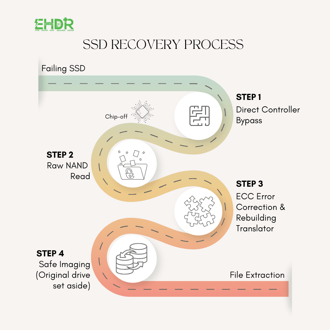
Step 1: Direct Controller Bypass
Recovery engineers attempt to communicate with the NAND chips directly through the existing controller. This bypasses corrupted firmware, damaged translation tables, or a partially failed controller while leaving the flash memory itself untouched.
- Diagnostic read of controller firmware state
- Attempt at vendor-specific service-mode or debug-port access
- Verification of whether the controller can still address the NAND array at all
This step is non-destructive and reversible. If it succeeds, later steps are unnecessary, which is why it’s always attempted first, even though it frequently fails on severely damaged drives.
Step 2: Chip-Off and Raw NAND Read
If the controller cannot reliably address the flash, engineers physically desolder the NAND chips (chip-off) and read them independently using specialized flash tools and programs.
- Precision desoldering under controlled heat profiles to avoid pad damage
- Direct pin-level or reballed reads of each NAND
- Extraction of completely raw, unstructured binary data with no file system, no logical order
Modern NAND uses multi-level cell (MLC/TLC/QLC) architecture, meaning each physical cell stores multiple bits with tight voltage thresholds. A single misread threshold can corrupt output, so reads are often repeated at multiple voltage references to maximize accuracy.
Step 3: ECC Error Correction and Translator Rebuilding
This is the step that consumes the most engineering time. Raw NAND data is not usable. It must be run through error correction and then reassembled using a reconstructed Flash Translation Layer (FTL).
- ECC correction: NAND flash inherently produces bit errors during read. Proprietary ECC algorithms must be replicated to correct them.
- FTL/mapping table rebuild: The controller’s logical-to-physical address mapping is reconstructed to put pages and blocks back into their correct logical order
Why this takes so long: Every SSD controller vendor uses a different, undocumented ECC and FTL scheme. There is no universal formula.
Step 4: Safe Imaging and File Extraction
Once data is decoded into a coherent structure, engineers create a full sector-by-sector image and set the original media aside permanently.
- Bit-for-bit image created on separate, verified storage
- All further work happens only on the image
- Original NAND chips/drive are archived untouched in case re-imaging is needed
Working exclusively from the image, protects against a second failure that would destroy the only copy of data.
SSD vs. HDD Recovery: Timeline Comparison
| Factor | HDD Recovery | SSD Recovery |
| Physical access to data | Direct (platters) | Indirect (via controller/NAND only) |
| Typical failure point | Mechanical (heads, motor) | Electronic/firmware (controller, NAND) |
| Data structure on read | Already ordered | Scrambled (wear-leveling, ECC-encoded) |
| Reconstruction needed | Minimal | FTL and ECC must be rebuilt |
| Typical turnaround | Hours to 1–2 days (If all platter,pcb in good condition with appropriate donor | Several days to weeks |
Immediate Risk-Mitigation Steps for IT Teams
If an SSD in your environment shows signs of failure (not detected in BIOS, sudden read-only mode, SMART errors, or the drive disappearing under load), the actions taken in the first hour matter more than any subsequent recovery step.
- Power down immediately: do not attempt repeated reboots or reseating, which can trigger further controller-level writes.
- Never run chkdsk, firmware updates, or “repair” utilities on a suspect SSD: these write to the drive and can overwrite recoverable NAND data.
- Do not attempt DIY chip-off: pad damage from improper desoldering is frequently unrecoverable even by professional labs
The Bottom Line
SSD recovery is slow because the drive’s controller is usually the very thing that failed. Every hour of “waiting” during a professional recovery is typically either precision chip-off work, ECC/FTL reverse-engineering, or verification imaging, not idle time. Understanding this process helps set realistic expectations and, more importantly, helps prevent well-intentioned DIY steps from turning a recoverable failure into a permanent data loss event.
If you're seeing any of these SSD failure symptoms right now, stop using the drive and contact us for a free diagnostic before attempting any fixes.
EHDR, We Leave No Data behind.